Overview
In this lesson, you will learn how to use 74HC595. 74HC595 consists of an 8−bit shift register and a storage register with three−state parallel outputs. It converts serial input into parallel output so you can save IO ports of an MCU.
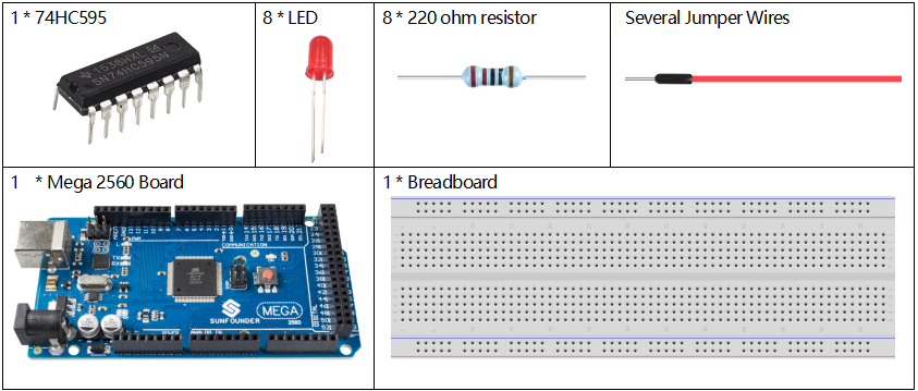
Components Required
Component Introduction
When MR (pin10) is high level and OE (pin13) is low level, data is input in the rising edge of SHcp and goes to the memory register through the rising edge of SHcp. If the two clocks are connected together, the shift register is always one pulse earlier than the memory register. There is a serial shift input pin (Ds), a serial output pin (Q) and an asynchronous reset button (low level) in the memory register. The memory register outputs a Bus with a parallel 8-bit and in three states. When OE is enabled (low level), the data in memory register is output to the bus.
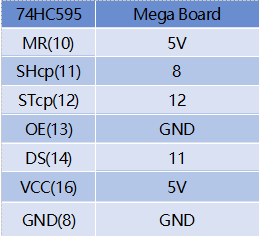
Pins of 74HC595 and their functions:
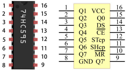
Q0-Q7: 8-bit parallel data output pins, able to control 8 LEDs or 8 pins of 7-segment display directly.
Q7’: Series output pin, connected to DS of another 74HC595 to connect multiple 74HC595s in series
MR: Reset pin, active at low level;
SHcp: Time sequence input of shift register. On the rising edge, the data in shift register moves successively one bit, i.e. data in Q1 moves to Q2, and so forth. While on the falling edge, the data in shift register remain unchanged.
STcp: Time sequence input of storage register. On the rising edge, data in the shift register moves into memory register.
OE: Output enable pin, active at low level.
DS: Serial data input pin
VCC: Positive supply voltage
GND: Ground
Fritzing Circuit
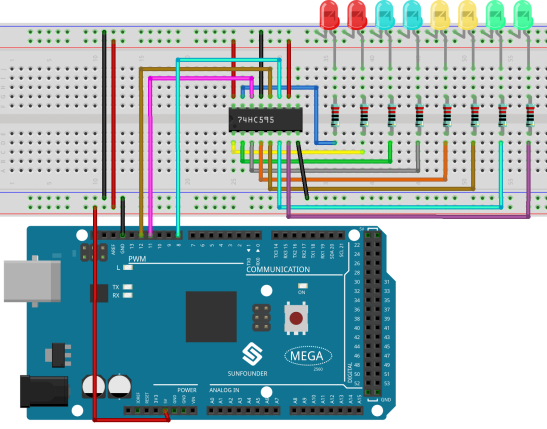
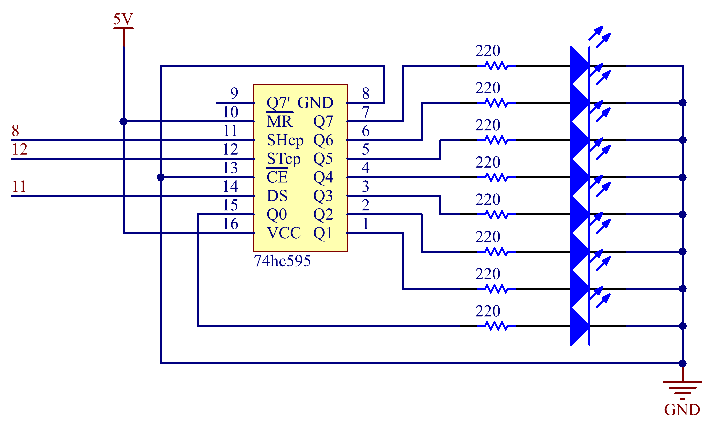
In this example, we use 74HC595 to control LED. Give each data output pin(Q0-Q7)a 220 ohm resistor then connect them to LED. The wiring diagram is as follows:
Schematic Diagram
Code
const int STcp = 12;//Pin connected to ST_CP of 74HC595
const int SHcp = 8; //Pin connected to SH_CP of 74HC595
const int DS = 11;  //Pin connected to DS of 74HC595
int datArray[] = {B00000000, B00000001, B00000011, B00000111, B00001111, B00011111, B00111111, B01111111, B11111111};

void setup()
{
  //set pins to output
  pinMode(STcp,OUTPUT);
  pinMode(SHcp,OUTPUT);
  pinMode(DS,OUTPUT);
}

void loop()
{
  for(int num = 0; num <=8; num++)
  {
    digitalWrite(STcp,LOW); //ground ST_CP and hold low for as long as you are transmitting
    shiftOut(DS,SHcp,MSBFIRST,datArray[num]);
    //return the latch pin high to signal chip that it
    //no longer needs to listen for information
    digitalWrite(STcp,HIGH); //pull the ST_CPST_CP to save the data
    delay(500); //wait for a second
  }
}
When you finish uploading the codes to the Mega2560 board, you can see the LEDs turning on one after another.
Code Analysis
Declare an array, store several 8 bit binary numbers that are used to change the working state of the eight LEDs controlled by 74HC595.
int datArray[] = {B00000000, B00000001, B00000011, B00000111, B00001111, B00011111, B00111111, B01111111, B11111111};Set STcp to low level first and then high level. It will generate a rising edge pulse of STcp.
digitalWrite(STcp,LOW); shiftOut() is used to shift out a byte of data one bit at a time, which means to shift a byte of data in datArray[num] to the shifting register with the DS pin. MSBFIRST means to move from high bits.
shiftOut(DS,SHcp,MSBFIRST,datArray[num]);After digitalWrite(STcp,HIGH) is run, the STcp will be at the rising edge. At this time, the data in the shift register will be moved to the memory register.
digitalWrite(STcp,HIGH);A byte of data will be transferred into the memory register after 8 times. Then the data of memory register are output to the bus (Q0-Q7). For example, shiftout「B00000001」will light up the LED controlled by Q0 and turn off the LED controlled by Q1~Q7.
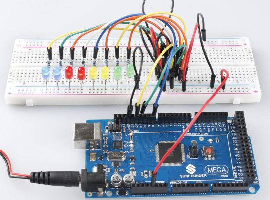
Phenomenon Picture