Introduction
In this experiment, you will learn how to use 74HC595 to drive a 7-segment display.
Generally, there are two ways to drive a single 7-segment display. One is to connect its 8 pins directly to eight ports on the SunFounder Uno board, which we have done previously. The other is to connect 74HC595 to three ports of the SunFounder Uno board and connect the 7-segment display to 74HC595. In this experiment, we will use the latter. By this way, you can save five ports. Considering the SunFounder Uno board’s limited ports, this is very important.
Components
– 8 * Resistor (220Ω)
– 1 * 74HC595
– 1 * SunFounder Uno board
– Jumper wires
– 1 * Breadboard
– 1 * USB cable
– 1 * 7-segment display
Principle
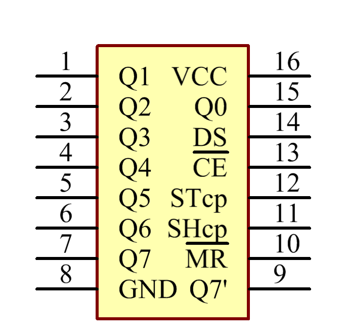
74HC595
The 74HC595 consists of an 8−bit shift register and a storage register with three−state parallel outputs. It converts serial input into parallel output so that you can save IO ports of an MCU. The 74HC595 is widely used to indicate multipath LEDs and drive multi-bit segment displays. “Three-state” refers to the fact that you can set the output pins as either high, low or “high impedance.” With data latching, the instant output will not be affected during the shifting; with data output, you can cascade 74HC595s more easily.

Pinsof 74HC595 and their functions:
Q0-Q7: 8-bit parallel data output pins, able to control 8 LEDs or 8 pins of 7-segment display directly.
Q7’: Series output pin, connected to DS of another 74HC595 to connect multiple 74HC595s in series
MR: Reset pin, active at low level; here it is directly connected to 5V.
SH: Time sequence input of shift register. On the rising edge, the data in shift register moves successively one bit, i.e. data in Q1 moves to Q2, and so forth. While on the falling edge, the data in shift register remain unchanged.
ST: Time sequence input of storage register. On the rising edge, data in the shift register moves into memory register.
OE : Output enable pin, active at low level, connected to GND.
Ds : Serial data input pin
VCC: Positive supply voltage
GND: Ground
Here the shiftout() function is used, which comes with the Arduino IDE. Simply input a number between 0 and 255 and the storage register can convert it into an 8-bit binary number and output it in parallel. This allows you to easily control the 8 pins of the 7-segment display and create any patterns you want.
Experimental Procedures
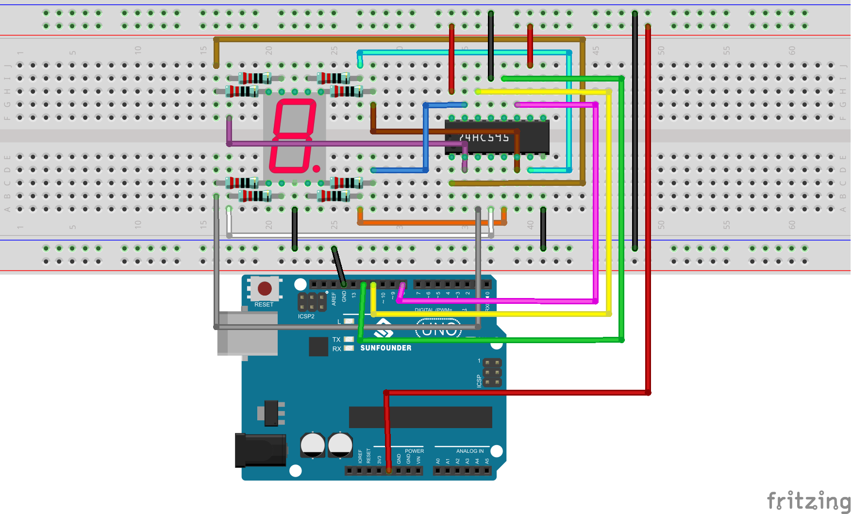
Step 1: Build the circuit
| 7-Segment Display | 74HC595 | SunFounder Uno R3 |
| a | Q7 | |
| b | Q6 | |
| c | Q5 | |
| d | Q4 | |
| e | Q3 | |
| f | Q2 | |
| g | Q1 | |
| DP | Q0 | |
| VCC | 5V | |
| DS | 11 | |
| CE | GND | |
| ST | 12 | |
| SH | 8 | |
| MR | 5V | |
| Q7’ | N/C | |
| GND | GND | |
| “ – ” | GND |

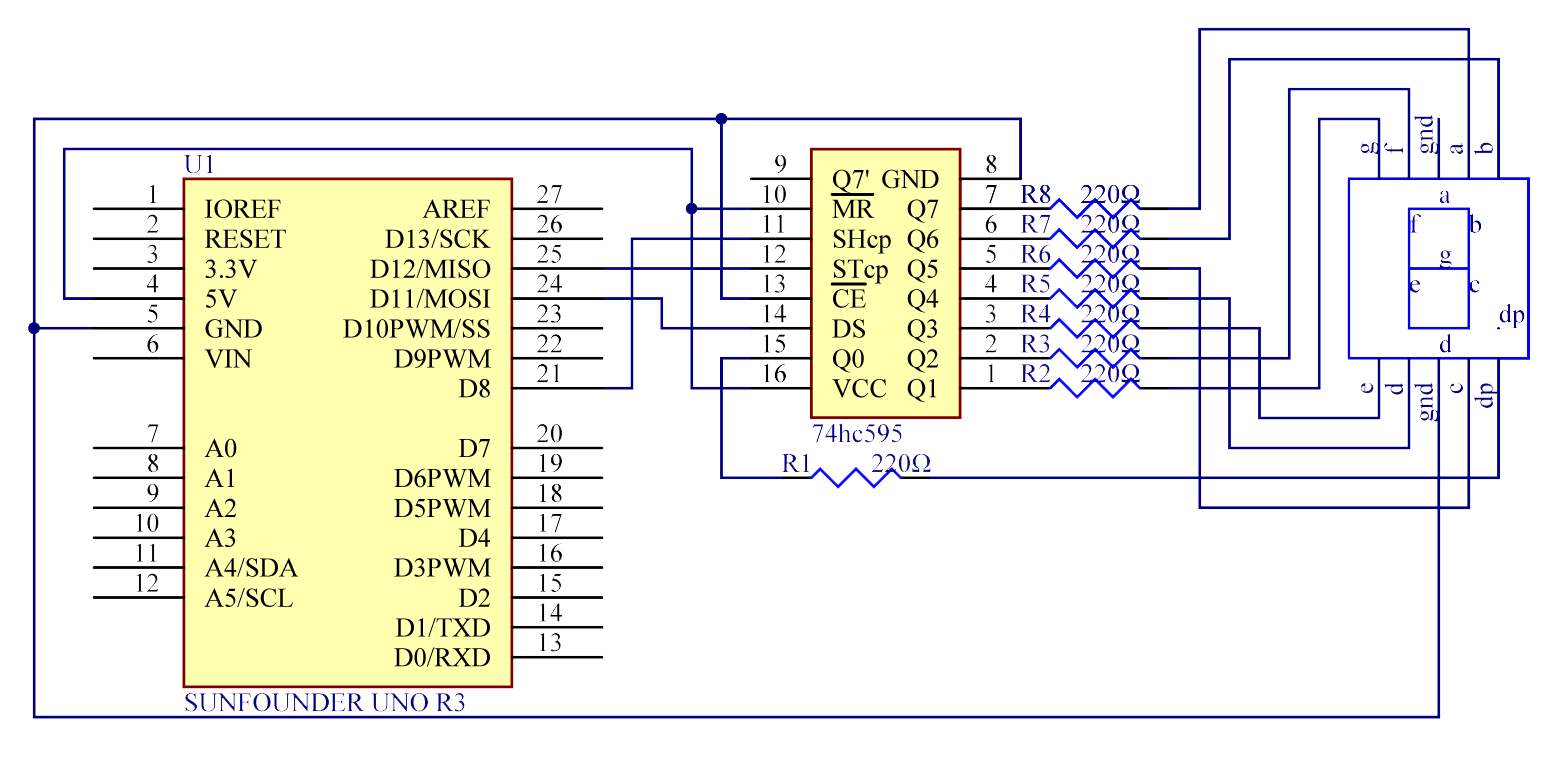
The schematic diagram

Step 2: Program (please go to our official website www.sunfounder.com to download related code by clicking LEARN -> Get Tutorials)
Step 3: Compile the program
Step 4: Burn the program into the SunFounder Uno board
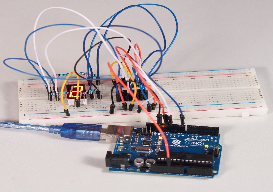
You should now see the 7-segment display cycle from 0 to F.

Code
| //74HC595//You should now be able to see the 7-segment display cycle from 0 to F //Email:support@sunfounder.com //Website:www.sunfounder.com //2015.5.7 const int latchPin = 12;//Pin 12 connected to ST_CP of 74HC595 const int clockPin = 8;//Pin 8 connected to SH_CP of 74HC595 const int dataPin = 11; //Pin 11 connected to DS of 74HC595 //display 0,1,2,3,4,5,6,7,8,9,A,b,C,d,E,F int datArray[16] = {252, 96, 218, 242, 102, 182, 190, 224, 254, 246, 238, 62, 156, 122, 158, 142}; void setup () { //set pins to output pinMode(latchPin,OUTPUT); pinMode(clockPin,OUTPUT); pinMode(dataPin,OUTPUT); } void loop() { for(int num = 0; num < 16; num++) { digitalWrite(latchPin,LOW); //ground latchPin and hold low for as long as you are transmitting shiftOut(dataPin,clockPin,MSBFIRST,datArray[num]); //return the latch pin high to signal chip that it //no longer needs to listen for information digitalWrite(latchPin,HIGH); //pull the latchPin to save the data delay(1000); //wait for a second } } |
Video
