Introduction
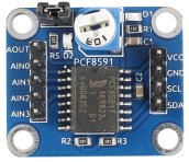
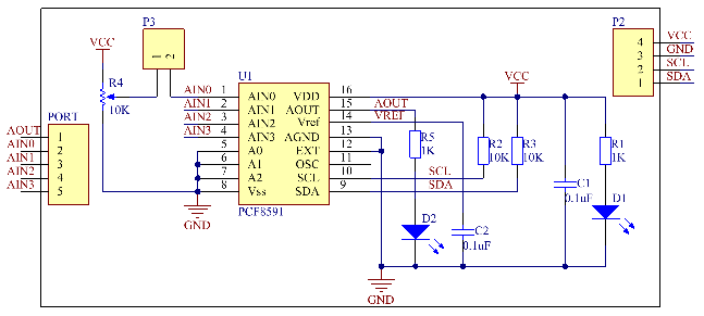
The PCF8591 is a single-chip, single-supply low-power 8-bit CMOS data acquisition device with four analog inputs, one analog output and a serial I2C-bus interface. Three address pins A0, A1 and A2 are used for programming the hardware address, allowing the use of up to eight devices connected to the I2C-bus without additional hardware. Address, control and data to and from the device are transferred serially via the two-line bidirectional I2C-bus.
The functions of the device include analog input multiplexing, on-chip track and hold function, 8-bit analog-to-digital conversion and an 8-bit digital-to-analog conversion. The maximum conversion rate is given by the maximum speed of the I2C-bus.
Required Components
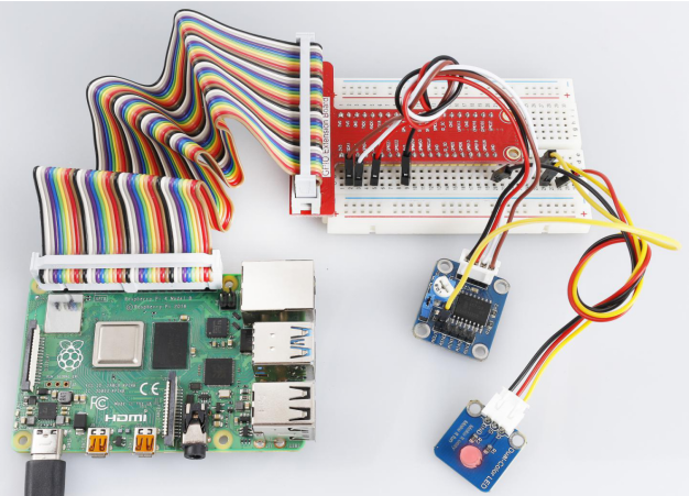
– 1 * Raspberry Pi
– 1 * Breadboard
– Several Jumper wires
– 1 * PCF8591 module
– 1 * Dual-Color LED module
– 1 * 3-Pin anti-reverse cable
Experimental Principle
Addressing:
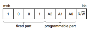
Each PCF8591 device in an I2C-bus system is activated by sending a valid address to the device. The address consists of a fixed part and a programmable part. The programmable part must be set according to the address pins A0, A1 and A2. The address always has to be sent as the first byte after the start condition in the I2C-bus protocol. The last bit of the address byte is the read/write-bit which sets the direction of the following data transfer (see as below).
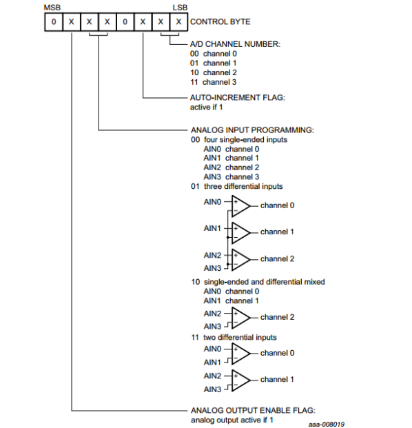
Control byte:
The second byte sent to a PCF8591 device will be stored in its control register and is required to control the device function. The upper nibble of the control register is used for enabling the analog output, and for programming the analog inputs as single-ended or differential inputs. The lower nibble selects one of the analog input channels defined by the upper nibble (see Fig.5). If the auto-increment flag is set, the channel number is incremented automatically after each A/D conversion. See the figure below.
In this experiment, the AIN0 (Analog Input 0) port is used to receive analog signals from the potentiometer module, and AOUT (Analog Output) is used to output analog signals to the dual-color LED module so as to change the luminance of the LED.
The schematic diagram:
Experimental Procedures
Step 1: Build the circuit.
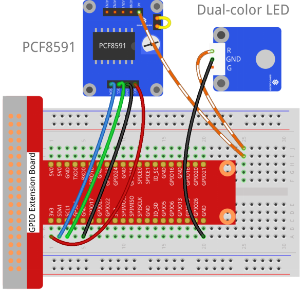
| Raspberry Pi | GPIO Extension Board | PCF8591 Module |
| SDA | SDA1 | SDA |
| SCL | SCL1 | SCL |
| 3.3V | 3V3 | VCC |
| GND | GND | GND |
| Dual-Color Module | GPIO Extension Board | PCF8591 Module |
| R | * | AOUT |
| GND | GND | GND |
| G | * | * |
Note:
Connect the two pins next to the potentiometer of the PCF8591 module with the jumper cap attached.
Step 2: Setup I2C (see Appendix. If you have set I2C, skip this step.)
For C Users:
Step 3: Change directory.
cd /home/pi/SunFounder_SensorKit_for_RPi2/C/13_pcf8591/Step 4: Compile.
gcc pcf8591.c -lwiringPiStep 5: Run.
sudo ./a.outFor Python Users:
Step 3: Change directory.
cd /home/pi/SunFounder_SensorKit_for_RPi2/Python/Step 4: Run.
sudo python3 13_pcf8591.pyNow, turn the knob of the potentiometer on PCF8591, and you can see the luminance of the LED change and a value between 0 and 255 printed on the screen.