Introduction
With low-voltage scanning, dot matrix LED displays have advantages such as power saving, long service life, low cost, high brightness, a wide angle of view, long visual range, waterproofness, and so on. They can meet the needs of different applications and thus have a broad development prospect. In this experiment, we will make it display some simple characters like numbers and letters to experience its charm from the beginning.
Components
– 1 * SunFounder Uno board
– 1 * Dot-matrix (8*8)
– 8 * Resistor (220Ω)
– 1 * Breadboard
– 2 * 74HC595
– 1 * USB cable
– Jumper wires
Principle
Dot Matrix
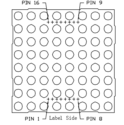
Generally, there are two types of dot matrix – common cathode and common anode. They look almost the same in appearance. But usually there will be labels for easy recognition. The one with a label ending with AX is a common cathode dot matrix and that with BX is a common anode one. See the figure below for how they look like. So the pins are distributed at the two ends of the matrix. Pins at one end (usually the label side) are 1-8 from left to right, when at the opposite they are 9-16 from right to left.
The external view:
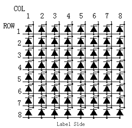
Below is the internal structure. You can see that in the common anode dot matrix, ROW is the anode of LED and COL is the cathode, while the situation in the common cathode one is opposite. Though for both types, the columns are the pin 13, 3, 4, 10, 6, 11, 15, and 16 and rows are the pin 9, 14, 8, 12, 1, 7, 2, and 5 in the dot matrix. To light up the first LED on the upper left corner, you need to set pin 9 as high level and pin 13 as low level in the common anode dot matrix; for a common cathode one, set pin 13 as high and pin 9 as low. If you want to turn on all the LEDs at the first row, in a common cathode dot matrix, set pin 13 as low level and ROW 9, 14, 8, 12, 1, 7, 2, and 5 as high level. In a common anode one, set pin 13 as high level and those rows as low level. See the figure below for better understanding.
The internal view:

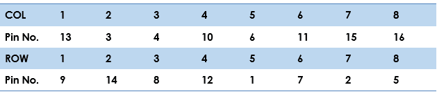
Pin numbering corresponding to the above rows and columns:
The schematic diagram
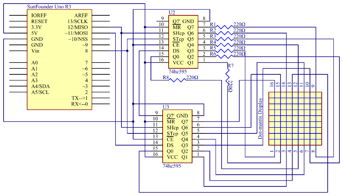
In this experiment, two 74HC595 chips are used – one to control the rows and the other, the columns. They are connected by cascading. The SHcp and STcp are shared between them. Connect pin DS of the U3 (see as above) to pin 11 of the Uno, and Q7′ of the U3 to DS of the U2 so the two chips are cascaded. Then when a 16-bit data is sent, the first 8 bits are transferred to the U3 and the rest 8 bits to the U2, thus controlling rows and columns of the dot matrix.
Experimental Procedures
Step 1: Build the circuit
Since the wiring of this experiment is a little complicated, we will do it step by step.
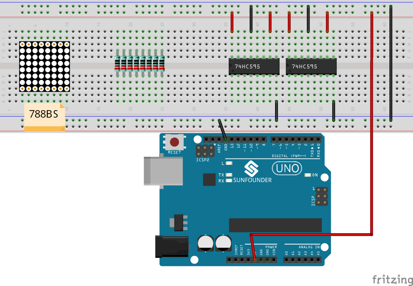
1) Insert all the devices needed into the breadboard. Then connect pin 16 and pin 10 of the 74HC595 to 5V of the control board, pin 8 and pin 13 to the GND. The 788BS on the image means you should put the matrix with the side marked with “788BS” facing that direction.
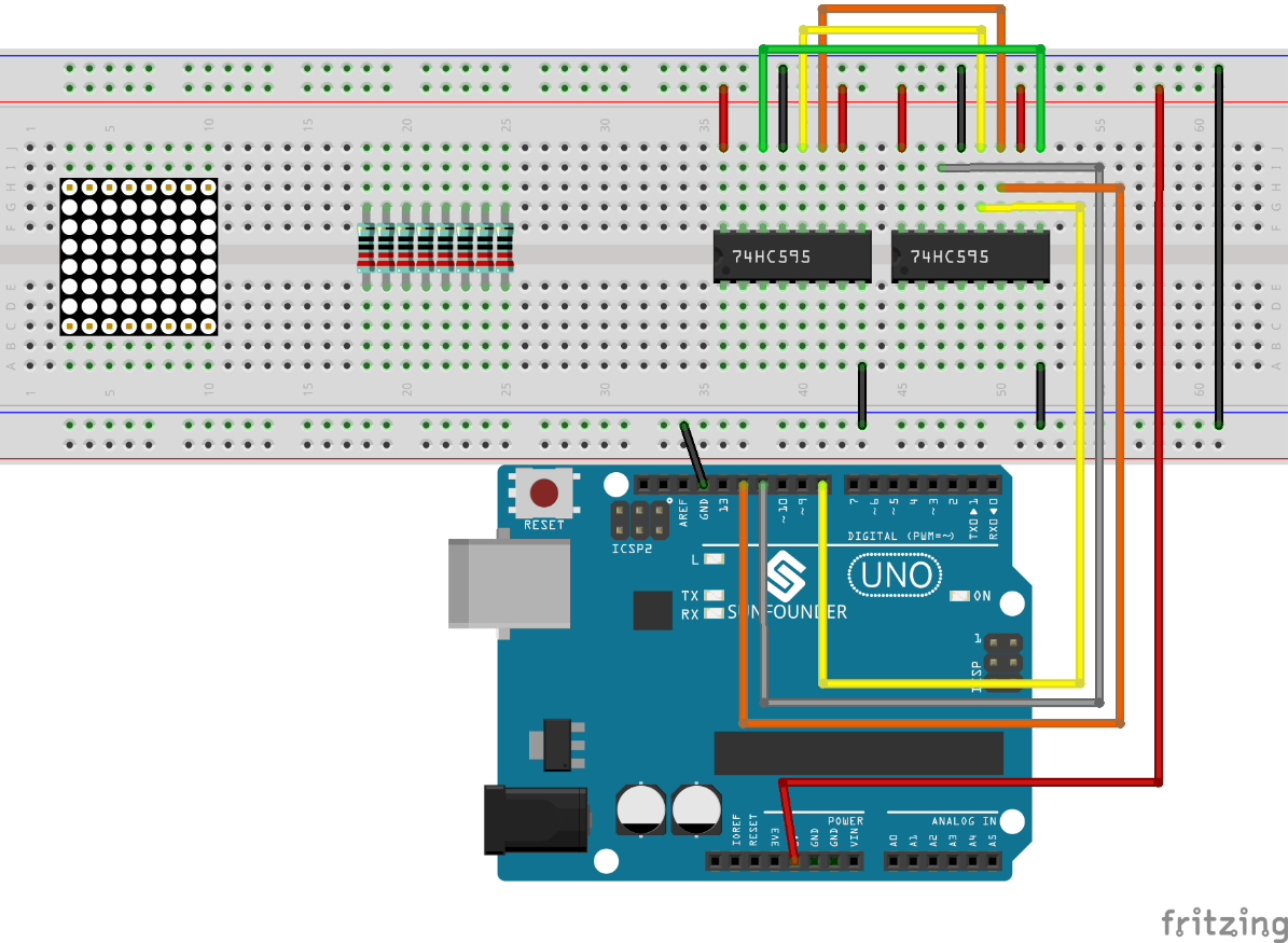
2) Connect pin 11 of the two 74HC595 chips together and connect them to pin 12 of the control board. Connect pin 12 of the two 74HC595 and then to pin 8. Pin 14 of the 74HC595 on the left connects to pin 9 on the right. Connect pin 14 of the 74HC595 on the right to the pin 11 of the control board.
3) The 74HC595 on the left controls the ROW of the dot matrix. To prevent burning the matrix, we need to connect a 220 ohm current limiting resistor to each row. Connect Q0-Q7 of the 74HC595 to pin 5, 2, 7, 1, 12, 8, 14, and 9 of the dot matrix.
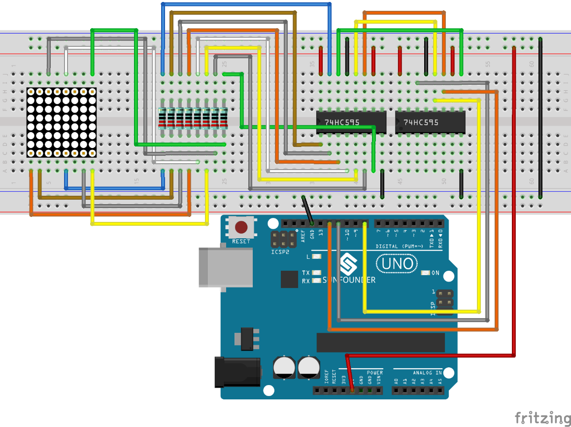
4) The 74HC595 on the right controls the columns of the matrix. Connect Q0-Q7 of the 74HC595 to pin 13, 3, 4, 10, 6, 11, 15, and 16 of the matrix respectively.

Step 2: Open the code file
Step 3: Select correct Board and Port
Step 4: Upload the sketch to the SunFounder Uno board
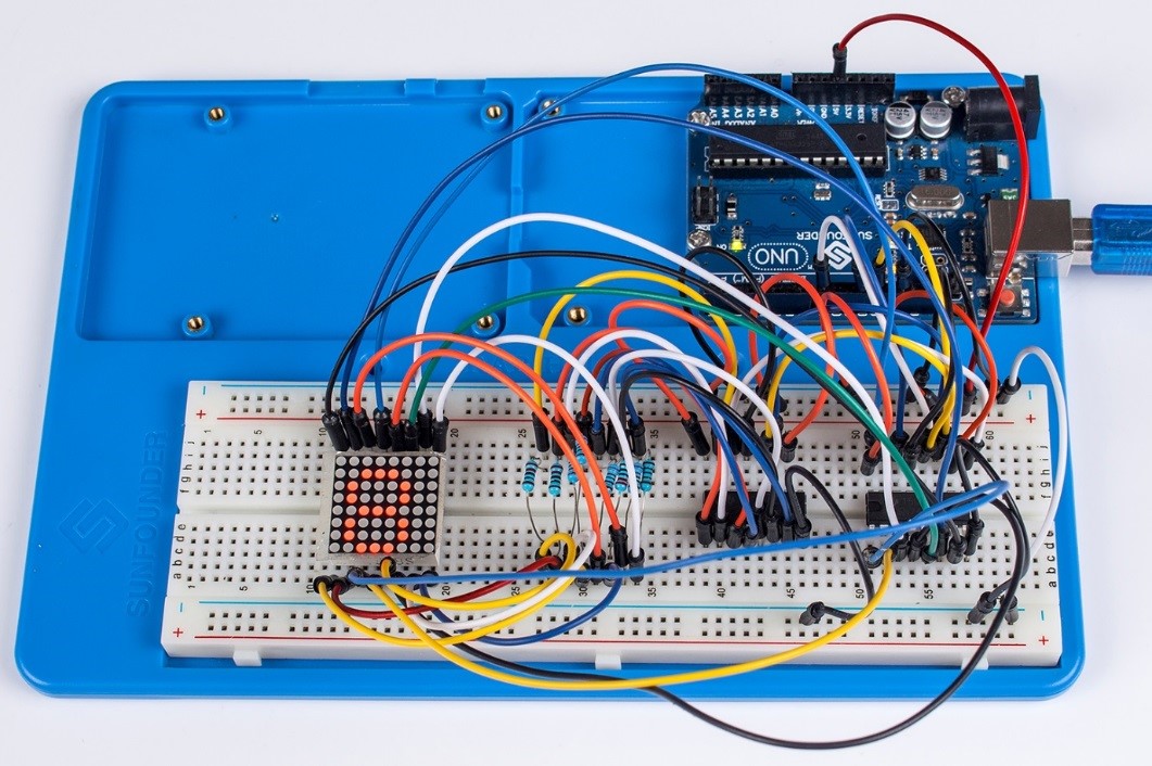
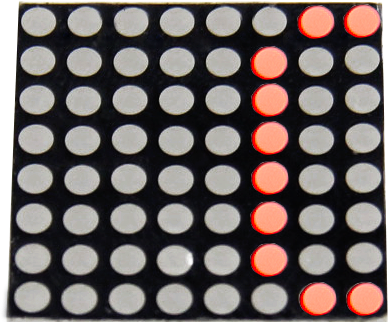
Here you should see the dot-matrix display 0 to 9 and then A to F circularly.

Before starting to write the code, you need to use a font software to get the dot patterns defining the characters to be displayed and store them in an array as the data[] shows.
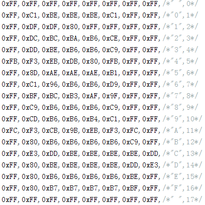
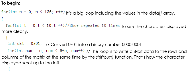
You can see that there are 18 rows in the array (the first and last rows are blank) x 8 columns = 144 hexadecimal numbers in total. In the array sorts, the numbers are sorted like this: 0~7 (the first row), 8~15 (the second row) and so on, till 135-143 (the last row).
This array is used to control the ROWs of the dot matrix – when the ROW is high level, the corresponding dots will brighten.
Now, let’s learn more about the array. Take the display of “0” as an example.

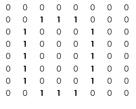
They are 8 hexadecimal numbers. Use a “~” (~data[num]), meaning inverting each number, and we can get 0x00, 0x3E, 0x41, 0x41, 0x41, 0x3E, 0x00, 0x00 after inverting the 8 numbers one by one. Convert the numbers into binary ones: 0000 0000, 0011 1110, 0100 0001, 0100 0001, 0100 0001, 0011 1110, 0000 0000, 0000 0000. Copy the arrays to the code and you will see 0 displayed in the dot matrix.

Procedures of the displaying: In the data[] array, first display data[0](0xFF) to data[7] (0xFF): blank in the matrix. Then data[1] (0xFF) to data[8] (0xFF): still blank. When it comes to data[2] (0xFF) to data[10](0xC1), it begins to display the left column of 0 (0011 1110). The rest goes the similar way. So we will see the matrix display the characters 0-F which scroll to the left. In order to show them clearly, repeat each display 10 times – see the for(int t = 0;t < 10;t ++).
Code
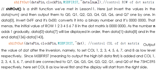
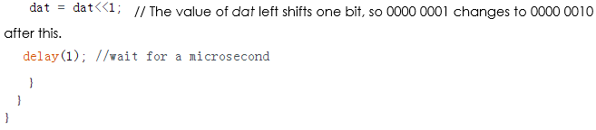
| //Dot-Matrix Display //The dot-matrix will display 0 to F circularly //Email:support@sunfounder.com //Website:www.sunfounder.com //2015.5.7 const int latchPin = 8;//Pin connected to ST_CP of 74HC595 const int clockPin = 12;//Pin connected to SH_CP of 74HC595 const int dataPin = 11; //Pin connected to DS of 74HC595 int data[] = { 0xFF,0xFF,0xFF,0xFF,0xFF,0xFF,0xFF,0xFF,/*” “,0*/ 0xFF,0xC1,0xBE,0xBE,0xBE,0xC1,0xFF,0xFF,/*”0″,1*/ 0xFF,0xDF,0xDF,0x80,0xFF,0xFF,0xFF,0xFF,/*”1″,2*/ 0xFF,0xDC,0xBC,0xBA,0xB6,0xCE,0xFF,0xFF,/*”2″,3*/ 0xFF,0xDD,0xBE,0xB6,0xB6,0xC9,0xFF,0xFF,/*”3″,4*/ 0xFB,0xF3,0xEB,0xDB,0x80,0xFB,0xFF,0xFF,/*”4″,5*/ 0xFF,0x8D,0xAE,0xAE,0xAE,0xB1,0xFF,0xFF,/*”5″,6*/ 0xFF,0xC1,0x96,0xB6,0xB6,0xD9,0xFF,0xFF,/*”6″,7*/ 0xFF,0xBF,0xBC,0xB3,0xAF,0x9F,0xFF,0xFF,/*”7″,8*/ 0xFF,0xC9,0xB6,0xB6,0xB6,0xC9,0xFF,0xFF,/*”8″,9*/ 0xFF,0xCD,0xB6,0xB6,0xB4,0xC1,0xFF,0xFF,/*”9″,10*/ 0xFC,0xF3,0xCB,0x9B,0xEB,0xF3,0xFC,0xFF,/*”A”,11*/ 0xFF,0x80,0xB6,0xB6,0xB6,0xB6,0xC9,0xFF,/*”B”,12*/ 0xFF,0xE3,0xDD,0xBE,0xBE,0xBE,0xBE,0xDD,/*”C”,13*/ 0xFF,0x80,0xBE,0xBE,0xBE,0xBE,0xDD,0xE3,/*”D”,14*/ 0xFF,0x80,0xB6,0xB6,0xB6,0xB6,0xBE,0xFF,/*”E”,15*/ 0xFF,0x80,0xB7,0xB7,0xB7,0xB7,0xBF,0xFF,/*”F”,16*/ 0xFF,0xFF,0xFF,0xFF,0xFF,0xFF,0xFF,0xFF,/*” “,17*/ }; void setup () { //set pins to output pinMode(latchPin,OUTPUT); pinMode(clockPin,OUTPUT); pinMode(dataPin,OUTPUT); } void loop() { for(int n = 0; n < 136; n++) { for(int t = 0;t < 10;t ++)//Show repeated 10 times { int dat = 0x01; for(int num = n; num < 8+n; num++) { shiftOut(dataPin,clockPin,MSBFIRST,~data[num]);//control ROW of dot matrix shiftOut(dataPin,clockPin,MSBFIRST,~dat); //control COL of dot matrix //return the latch pin high to signal chip that it //no longer needs to listen for information digitalWrite(latchPin,HIGH); //pull the latchPin to save the data //delay(1); //wait for a microsecond digitalWrite(latchPin,LOW); //ground latchPin and hold low for as long as you are transmitting dat = dat< < 1; delay(1); //wait for a microsecond } } } } |