Introduction
The ADC function can be used to convert analog signals to digital signals, and in this experiment, ADC0834 is used to get the function involving ADC. Here, we implement this process by using potentiometer. Potentiometer changes the physical quantity — voltage, which is converted by the ADC function.
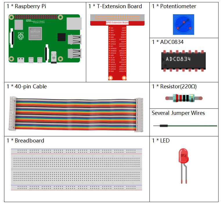
Components
Principle
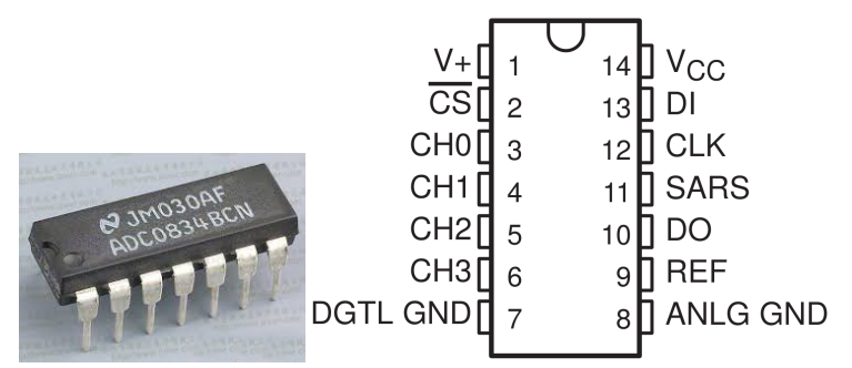
ADC0834
ADC0834 is an 8-bitsuccessive approximation analog-to-digital converter that is equipped with an input-configurable multichannel multi-plexer and serial input/output. The serial input/output is configured to interface with standard shift registers or microprocessors.
Sequence of Operation
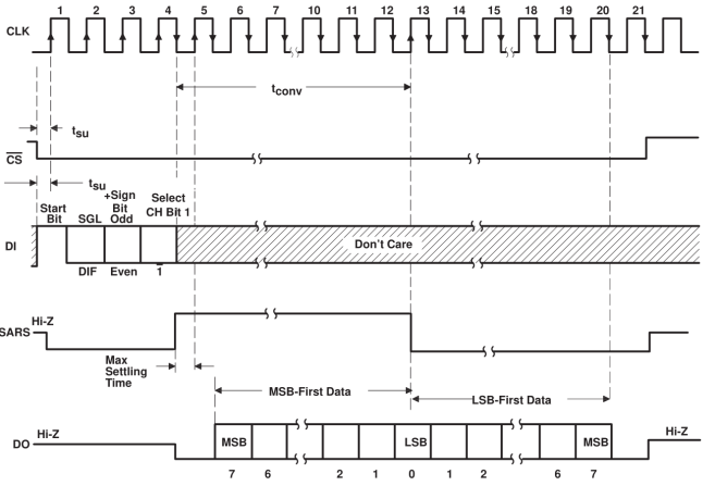
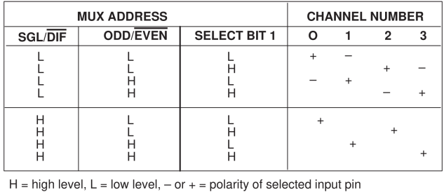
A conversion is initiated by setting CS low, which enables all logic circuits. CS must be held low for the complete conversion process. A clock input is then received from the processor. On each low-to-high transition of the clock input, the data on DI is clocked into the multiplexer address shift register. The first logic high on the input is the start bit. A 3- to 4-bit assignment word follows the start bit. On each successive low-to-high transition of the clock input, the start bit and assignment word are shifted through the shift register. When the start bit is shifted into the start location of the multiplexer register, the input channel is selected and conversion starts. The SAR Statu output (SARS) goes high to indicate that a conversion is in progress, and DI to the multiplexer shift register is disabled the duration of the conversion.
An interval of one clock period is automatically inserted to allow the selected multiplexed channel to settle. The data output DO comes out of the high-impedance state and provides a leading low for this one clock period of multiplexer settling time. The SAR comparator compares successive outputs from the resistive ladder with the incoming analog signal. The comparator output indicates whether the analog input is greater than or less than the resistive ladder output. As the conversion proceeds, conversion data is simultaneously output from the DO output pin, with the most significant bit (MSB) first.
After eight clock periods, the conversion is complete and the SARS output goes low. Finally outputs the least-significant-bit-first data after the MSB-first data stream.
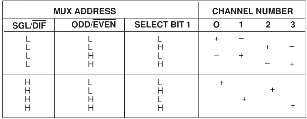
ADC0834 MUX ADDRESS CONTROL LOGIC TABLE
Potentiometer
Potentiometer is also a resistance component with 3 terminals and its resistance value can be adjusted according to some regular variation. Potentiometer usually consists of resistor and movable brush. When the brush is moving along the resistor, there is a certain resistance or voltage output depending on the displacement.
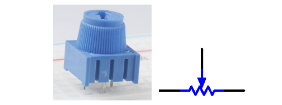
The functions of the potentiometer in the circuit are as follows:
1. Serving as a voltage divider
Potentiometer is a continuously adjustable resistor. When you adjust the shaft or sliding handle of the potentiometer, the movable contact will slide on the resistor. At this point, a voltage can be output depending on the voltage applied onto the potentiometer and the angle the movable arm has rotated to or the distance it moves.
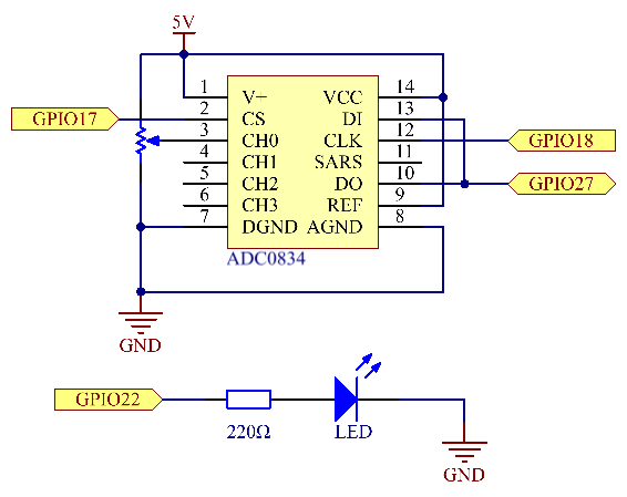
Schematic Diagram
| T-Board Name | physical | wiringPi | BCM |
| GPIO17 | Pin 11 | 0 | 17 |
| GPIO18 | Pin 12 | 1 | 18 |
| GPIO27 | Pin 13 | 2 | 27 |
| GPIO22 | Pin15 | 3 | 22 |
Experimental Procedures
Step 1: Build the circuit.
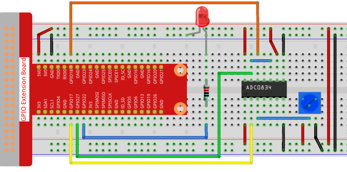
Note: Please place the chip by referring to the corresponding position depicted in the picture. Note that the grooves on the chip should be on the left when it is placed.
- For C Language Users
Step 2: Open the code file.
cd /home/pi/davinci-kit-for-raspberry-pi/c/2.1.4/Step 3: Compile the code.
gcc 2.1.4_Potentiometer.c -lwiringPiStep 4: Run.
sudo ./a.outAfter the code runs, rotate the knob on the potentiometer, the intensity of LED will change accordingly.
Code
#include <wiringPi.h>
#include <stdio.h>
#include <softPwm.h>

typedef unsigned char uchar;
typedef unsigned int uint;

#define     ADC_CS    0
#define     ADC_CLK   1
#define     ADC_DIO   2
#define     LedPin    3

uchar get_ADC_Result(uint channel)
{
    uchar i;
    uchar dat1=0, dat2=0;
    int sel = channel > 1 & 1;
    int odd = channel & 1;

    pinMode(ADC_DIO, OUTPUT);
    digitalWrite(ADC_CS, 0);
    // Start bit
    digitalWrite(ADC_CLK,0);
    digitalWrite(ADC_DIO,1);    delayMicroseconds(2);
    digitalWrite(ADC_CLK,1);    delayMicroseconds(2);
   //Single End mode
    digitalWrite(ADC_CLK,0);
    digitalWrite(ADC_DIO,1);    delayMicroseconds(2);
    digitalWrite(ADC_CLK,1);    delayMicroseconds(2);
    // ODD
    digitalWrite(ADC_CLK,0);
    digitalWrite(ADC_DIO,odd);  delayMicroseconds(2);
    digitalWrite(ADC_CLK,1);    delayMicroseconds(2);
    //Select
    digitalWrite(ADC_CLK,0);
    digitalWrite(ADC_DIO,sel);    delayMicroseconds(2);
    digitalWrite(ADC_CLK,1);

    digitalWrite(ADC_DIO,1);    delayMicroseconds(2);
    digitalWrite(ADC_CLK,0);
    digitalWrite(ADC_DIO,1);    delayMicroseconds(2);

    for(i=0;i<8;i++)
    {
        digitalWrite(ADC_CLK,1);    delayMicroseconds(2);
        digitalWrite(ADC_CLK,0);    delayMicroseconds(2);

        pinMode(ADC_DIO, INPUT);
        dat1=dat1<<1 | digitalRead(ADC_DIO);
    }

    for(i=0;i<8;i++)
    {
        dat2 = dat2 | ((uchar)(digitalRead(ADC_DIO))<<i);
        digitalWrite(ADC_CLK,1);    delayMicroseconds(2);
        digitalWrite(ADC_CLK,0);    delayMicroseconds(2);
    }

    digitalWrite(ADC_CS,1);
    pinMode(ADC_DIO, OUTPUT);
    return(dat1==dat2) ? dat1 : 0;
}

int main(void)
{
    uchar analogVal;
    if(wiringPiSetup() == -1){ //when initialize wiring failed,print messageto screen
        printf("setup wiringPi failed !");
        return 1;
    }
    softPwmCreate(LedPin,  0, 100);
    pinMode(ADC_CS,  OUTPUT);
    pinMode(ADC_CLK, OUTPUT);

    while(1){
        analogVal = get_ADC_Result(0);
        printf("Current analogVal : %d\n", analogVal);
        softPwmWrite(LedPin, analogVal);
        delay(100);
    }
    return 0;
}
Code Explanation
#define     ADC_CS    0
#define     ADC_CLK   1
#define     ADC_DIO   2
#define     LedPin    3
Define CS, CLK, DIO of ADC0834, and connect them to GPIO0, GPIO1 and GPIO2 respectively. Then attach LED to GPIO3.
uchar get_ADC_Result(uint channel)
{
    uchar i;
    uchar dat1=0, dat2=0;
    int sel = channel > 1 & 1;
    int odd = channel & 1;

    pinMode(ADC_DIO, OUTPUT);
    digitalWrite(ADC_CS, 0);
    // Start bit
    digitalWrite(ADC_CLK,0);
    digitalWrite(ADC_DIO,1);    delayMicroseconds(2);
    digitalWrite(ADC_CLK,1);    delayMicroseconds(2);
   //Single End mode
    digitalWrite(ADC_CLK,0);
    digitalWrite(ADC_DIO,1);    delayMicroseconds(2);
    digitalWrite(ADC_CLK,1);    delayMicroseconds(2);
    // ODD
    digitalWrite(ADC_CLK,0);
    digitalWrite(ADC_DIO,odd);  delayMicroseconds(2);
    digitalWrite(ADC_CLK,1);    delayMicroseconds(2);
    //Select
    digitalWrite(ADC_CLK,0);
    digitalWrite(ADC_DIO,sel);    delayMicroseconds(2);
    digitalWrite(ADC_CLK,1);

    digitalWrite(ADC_DIO,1);    delayMicroseconds(2);
    digitalWrite(ADC_CLK,0);
    digitalWrite(ADC_DIO,1);    delayMicroseconds(2);
    for(i=0;i<8;i++)
    {
        digitalWrite(ADC_CLK,1);    delayMicroseconds(2);
        digitalWrite(ADC_CLK,0);    delayMicroseconds(2);

        pinMode(ADC_DIO, INPUT);
        dat1=dat1<<1 | digitalRead(ADC_DIO);
    }

    for(i=0;i<8;i++)
    {
        dat2 = dat2 | ((uchar)(digitalRead(ADC_DIO))<<i);
        digitalWrite(ADC_CLK,1);    delayMicroseconds(2);
        digitalWrite(ADC_CLK,0);    delayMicroseconds(2);
    }

    digitalWrite(ADC_CS,1);
    pinMode(ADC_DIO, OUTPUT);
    return(dat1==dat2) ? dat1 : 0;
}
There is a function of ADC0834 to get Analog to Digital Conversion. The specific workflow is as follows:
digitalWrite(ADC_CS, 0);Set CS to low level and start enabling AD conversion.
// Start bit
digitalWrite(ADC_CLK,0);
digitalWrite(ADC_DIO,1);    delayMicroseconds(2);
digitalWrite(ADC_CLK,1);    delayMicroseconds(2);
When the low-to-high transition of the clock input occurs at the first time, set DIO to 1 as Start bit. In the following three steps, there are 3 assignment words.
//Single End mode
    digitalWrite(ADC_CLK,0);
    digitalWrite(ADC_DIO,1);    delayMicroseconds(2);
    digitalWrite(ADC_CLK,1);    delayMicroseconds(2);
As soon as the low-to-high transition of the clock input occurs for the second time, set DIO to 1 and choose SGL mode.
// ODD
digitalWrite(ADC_CLK,0);
digitalWrite(ADC_DIO,odd);  delayMicroseconds(2);
digitalWrite(ADC_CLK,1);    delayMicroseconds(2);
Once occurs for the third time, the value of DIO is controlled by the variable odd.
//Select
digitalWrite(ADC_CLK,0);
digitalWrite(ADC_DIO,sel);    delayMicroseconds(2);
digitalWrite(ADC_CLK,1);
The pulse of CLK converted from low level to high level for the forth time, the value of DIO is controlled by the variable sel.
Under the condition that channel=0, sel=0, odd=0, the operational formulas concerning sel and odd are as follows:
  int sel = channel > 1 & 1;
  int odd = channel & 1;
When the condition that channel=1, sel=0, odd=1 is met, please refer to the following address control logic table. Here CH1 is chosen, and the start bit is shifted into the start location of the multiplexer register and conversion starts.
digitalWrite(ADC_DIO,1);    delayMicroseconds(2);
digitalWrite(ADC_CLK,0);
digitalWrite(ADC_DIO,1);    delayMicroseconds(2);
Here, set DIO to 1 twice, please ignore it.
for(i=0;i<8;i++)
    {
        digitalWrite(ADC_CLK,1);    delayMicroseconds(2);
        digitalWrite(ADC_CLK,0);    delayMicroseconds(2);

        pinMode(ADC_DIO, INPUT);
        dat1=dat1<<1 | digitalRead(ADC_DIO);
    }
In the first for() statement, as soon as the fifth pulse of CLK is converted from high level to low level, set DIO to input mode. Then the conversion starts and the converted value is stored in the variable dat1. After eight clock periods, the conversion is complete.
for(i=0;i<8;i++)
    {
        dat2 = dat2 | ((uchar)(digitalRead(ADC_DIO))<<i);
        digitalWrite(ADC_CLK,1);    delayMicroseconds(2);
        digitalWrite(ADC_CLK,0);    delayMicroseconds(2);
    }
In the second for() statement, output the converted values via DO after other eight clock periods and store them in the variable dat2.
digitalWrite(ADC_CS,1);
pinMode(ADC_DIO, OUTPUT);
return(dat1==dat2) ? dat1 : 0;
return(dat1==dat2) ? dat1 : 0 is used to compare the value gotten during the conversion and the output value. If they are equal to each other, output the converting value dat1; otherwise, output 0. Here, the workflow of ADC0834 is complete.
softPwmCreate(LedPin, 0, 100);The function is to use software to create a PWM pin, LedPin, then the initial pulse width is set to 0, and the period of PWM is 100 x 100us.
while(1){
        analogVal = get_ADC_Result(0);
        printf("Current analogVal : %d\n", analogVal);
        softPwmWrite(LedPin, analogVal);
        delay(100);
    }
In the main program, read the value of channel 0 that has been connected with a potentiometer. And store the value in the variable analogVal then write it in LedPin. Now you can see the brightness of LED changing with the value of the potentiometer.
- For Python Users
Step 2: Open the code file
cd /home/pi/davinci-kit-for-raspberry-pi/python/Step 3: Run.
sudo python3 2.1.4_Potentiometer.pyAfter the code runs, rotate the knob on the potentiometer, the intensity of LED will change accordingly.
Code
#!/usr/bin/env python3

import RPi.GPIO as GPIO
import ADC0834
import time

LedPin = 22

def setup():
    global led_val
    # Set the GPIO modes to BCM Numbering
    GPIO.setmode(GPIO.BCM)
    # Set all LedPin's mode to output and initial level to High(3.3v)
    GPIO.setup(LedPin, GPIO.OUT, initial=GPIO.HIGH)
    ADC0834.setup()
    # Set led as pwm channel and frequece to 2KHz
    led_val = GPIO.PWM(LedPin, 2000)

    # Set all begin with value 0
    led_val.start(0)

# Define a MAP function for mapping values.  Like from 0~255 to 0~100
def MAP(x, in_min, in_max, out_min, out_max):
    return (x - in_min) * (out_max - out_min) / (in_max - in_min) + out_min

def destroy():
    # Stop all pwm channel
    led_val.stop()
    # Release resource
    GPIO.cleanup()

def loop():
    while True:
        res = ADC0834.getResult()
        print ('res = %d' % res)
        R_val = MAP(res, 0, 255, 0, 100)
        led_val.ChangeDutyCycle(R_val)
        time.sleep(0.2)

if __name__ == '__main__':
    setup()
    try:
        loop()
    except KeyboardInterrupt: # When 'Ctrl+C' is pressed, the program destroy() will be executed.
        destroy()
Code Explanation
import ADC0834import ADC0834 library. You can check the content of the library by calling the command nano ADC0834.py.
def setup():
    global led_val
    # Set the GPIO modes to BCM Numbering
    GPIO.setmode(GPIO.BCM)
    # Set all LedPin's mode to output and initial level to High(3.3v)
    GPIO.setup(LedPin, GPIO.OUT, initial=GPIO.HIGH)
    ADC0834.setup()
    # Set led as pwm channel and frequece to 2KHz
    led_val = GPIO.PWM(LedPin, 2000)

    # Set all begin with value 0
    led_val.start(0)
In setup(), define the naming method as BCM, set LedPin as PWM channel and render it a frequency of 2Khz.
ADC0834.setup(): Initialize ADC0834, and connect the defined CS, CLK, DIO of ADC0834 to GPIO17, GPIO18 and GPIO27 respectively.
def loop():
    while True:
        res = ADC0834.getResult()
        print ('res = %d' % res)
        R_val = MAP(res, 0, 255, 0, 100)
        led_val.ChangeDutyCycle(R_val)
        time.sleep(0.2)
The function getResult() is used to read the analog values of the four channels of ADC0834. By default, the function reads the value of CH0, and if you want to read other channels, please input the channel number in ( ), ex. getResult(1).
The function loop() first reads the value of CH0, then assign the value to the variable res. After that, call the function MAP to map the read value of potentiometer to 0~100. This step is used to control the duty cycle of LedPin. Now, you may see that the brightness of LED is changing with the value of potentiometer.
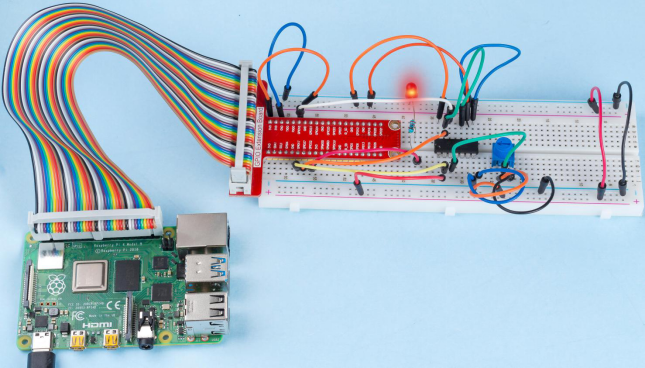
Phenomenon Picture